Optimizing FPGA-based Accelerator Design for Deep Convolutional Neural Networks
Main Issue
How to optimize FPGA-based Deep Neural Network (DNN) accelerator in terms of loop manipulation? And how does Roofline Model affect to performance in FPGA design?
Why FPGA?
FPGA (Field Prgrammable Gate Array) is powerful development platform to design specific purpose of hardware. Previously, FPGA was used to prototyping for ASIC (Application Specific Integrated Circuit). But, the performance improvement of FPGA can lead FPGA to real application field.
These days, GPU (Graphics Processing Unit) is most popular processor to run DNN. But GPU is for general purpose processor rather than various structure of DNNs. In that, FPGA’s reconfigurablility can support various DNN hardware. And programablility can support rapid design for DNN accelerator.
Before Read
Convolutional Neural Network (CNN)
CNN is kinds of DNN. CNN is usually used in image processing (e.g. image classification, object detection, image recognition). Basically, when people recognize image, the eyes trace many parts of image. For example, when we see the picture of dog, we see the dog’s eye, nose and mouth separately and finally we recognize a dog in that picture to combine those informations.
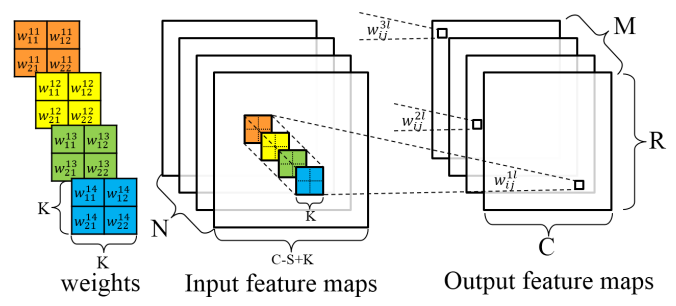
CNN consists of 2 parts, convolution and classify and there are many layers of both 2 in CNN. In convolution part, CNN extracts the features from the picture. there are input feature map, kernel and output feature map. Input feature map is the input images to convolution layer. Kernel is collection of features to detect. Convolution layer can collect the feature from input feature map using kernel. Output feature map is results of convolution layer from convolution process between input feature map and kernel. Output feature map is used as input feature map in the next layer.
Figure 1 in Optimizing FPGA-based Accelerator Design for Deep Convolutional Neural Networks, Chen Zhang et al. FPGA 2015
Roofline Model
There are 2 main points we should focus on when we design the DNN accelerator, computation and communication. Computation means the maximum performance the hardware(i.e. accelerator) can make. That means, the accelerator we design has performance bound.
Communication means the bandwidth between memory and computation units. Even though the performance bound is high, the actual performance is too low because of communication. Simply to say, there is not enough data feeding from memory to computation units.
Figure 3 in Optimizing FPGA-based Accelerator Design for Deep Convolutional Neural Networks, Chen Zhang et al. FPGA 2015
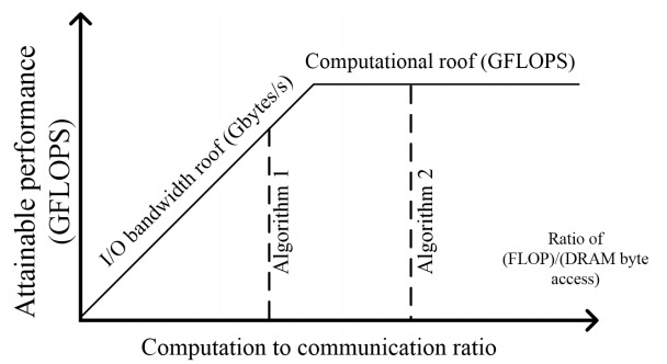
In the figure above, there are 2 Algorithms for example. The Algorithm 1 cannot exploit full performance because of not enough bandwidth. The Algorithm 2 cannot utilize full bandwidth because of performance bound. As a result, Attainable Performance in Roofline Model is like below:
Equation (1) in Optimizing FPGA-based Accelerator Design for Deep Convolutional Neural Networks, Chen Zhang et al. FPGA 2015
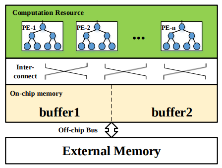
Accelerator Design
The CNN accelerator has some components, PE (Processing Element), On-chip Buffer, External Memory and On / Off-chip interconnect. At the beginning of process, all of data for input feature map and kernel are in External Memory. As proceeding the convolution layer, the data is fed from External Memory to On-chip Memory and from On-chip Memory to PEs. The On-chip Memory is used as cache in this architecture to reduce data access latency from External Memory. But, because the size of On-chip Memory is limited, the locality and data reuse should be considered carefully.
Figure 4 in Optimizing FPGA-based Accelerator Design for Deep Convolutional Neural Networks, Chen Zhang et al. FPGA 2015
Loop Manipulation
The basic loop statements of CNN is like below:
for ( row = 0 ; row < R ; row++ )
    for ( col = 0 ; col < C ; col++ )
        for ( oc = 0 ; oc < M ; oc++ )
            for ( ic = 0 ; ic < N ; ic++ )
                for ( kh = 0 ; kh < K ; kh++ )
                    for ( kw = 0 ; kw < K ; kw++ )
                        output[oc][col][row] += input[ic][col*S+kh][row*S+kw]
                        						* kernel[oc][ic][kh][kw];
There is less size of On-chip Memory, we should chop the feature maps. We call this process Tiling. After the tiling, the loop statements are changed:
// External Memory transfer
for ( row = 0 ; row < R ; row += Tr )
    for ( col = 0 ; col < C ; col += Tc )
        for ( oc = 0 ; oc < M ; oc += Tm )
            for ( ic = 0 ; ic < N ; ic += Tn )
            // Load input feature maps
            // Load kernels
            // Load output feature map partial sums

                // On-chip Memory computation
                for ( trr = row ; trr < min(row+Tr, R) ; trr++ )
                    for ( tcc = col ; tcc < min(col+Tc, C) ; tcc++ )
                        for ( occ = oc ; occ < min(oc+Tm, M) ; occ++ )
                            for ( icc = ic ; icc < min(ic+Tn, N) ; icc++ )
                                for ( kh = 0 ; kh < K ; kh++ )
                                    for ( kw = 0 ; kw < K ; kw++ )
                                        output[occ][tcc][trr] +=
                                        	input[icc][tcc*S+kh][trr*S+kw]
                                        	* kernel[occ][icc][kh][kw];
			// Store output feature map partial sums
We can change the sequence of loops in On-chip Memory computation: Loop Interchange.
// On-chip Memory computation
for ( kh = 0 ; kh < K ; kh++ )
	for ( kw = 0 ; kw < K ; kw++ )
		for ( trr = row ; trr < min(row+Tr, R) ; trr++ )
			for ( tcc = col ; tcc < min(col+Tc, C) ; tcc++ )
    			for ( occ = oc ; occ < min(oc+Tm, M) ; occ++ )
        			for ( icc = ic ; icc < min(ic+Tn, N) ; icc++ )
                    	output[occ][tcc][trr] += input[icc][tcc*S+kh][trr*S+kw]
                    								* kernel[occ][icc][kh][kw];
Loop Unrolling
We can unroll some loops to parallelize the computations.
// On-chip Memory computation
for ( kh = 0 ; kh < K ; kh++ )
	for ( kw = 0 ; kw < K ; kw++ )
		for ( trr = row ; trr < min(row+Tr, R) ; trr++ )
			for ( tcc = col ; tcc < min(col+Tc, C) ; tcc++ )
    			for ( occ = oc ; occ < min(oc+Tm, M) ; occ++ )
                #pragma HLS_UNROLL
        			for ( icc = ic ; icc < min(ic+Tn, N) ; icc++ )
                    #pragma HLS_UNROLL
                    	output[occ][tcc][trr] += input[icc][tcc*S+kh][trr*S+kw]
                    								* kernel[occ][icc][kh][kw];
The hardware implementations depend on the dependency between iterator which is unrolled and data.
Table 2 in Optimizing FPGA-based Accelerator Design for Deep Convolutional Neural Networks, Chen Zhang et al. FPGA 2015
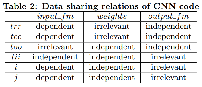
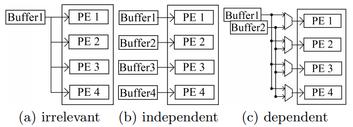
Let’s see the each case. First, the input feature map has irrelevant dependency with occ and independent dependency with icc. Second, the kernel has independent dependency both occ and icc. Third, the output feature map has independent dependency with occ and irrelevant dependency with icc. For each cases, the hardware implementations are different.
Figure 6 in Optimizing FPGA-based Accelerator Design for Deep Convolutional Neural Networks, Chen Zhang et al. FPGA 2015
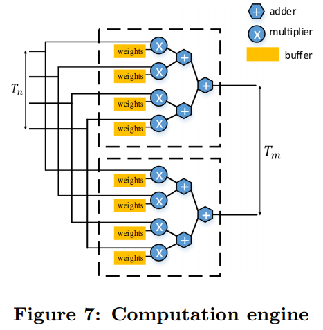
So, the overall hardware implementation for the computation engine is like below:
Figure 7 in Optimizing FPGA-based Accelerator Design for Deep Convolutional Neural Networks, Chen Zhang et al. FPGA 2015
Loop Pipelining
We can pipeline the loop to improve throughput.
// On-chip Memory computation
for ( kh = 0 ; kh < K ; kh++ )
	for ( kw = 0 ; kw < K ; kw++ )
		for ( trr = row ; trr < min(row+Tr, R) ; trr++ )
			for ( tcc = col ; tcc < min(col+Tc, C) ; tcc++ )
            #pragma HLS_PIPELINE
    			for ( occ = oc ; occ < min(oc+Tm, M) ; occ++ )
                #pragma HLS_UNROLL
        			for ( icc = ic ; icc < min(ic+Tn, N) ; icc++ )
                    #pragma HLS_UNROLL
                    	output[occ][tcc][trr] += input[icc][tcc*S+kh][trr*S+kw]
                    								* kernel[occ][icc][kh][kw];
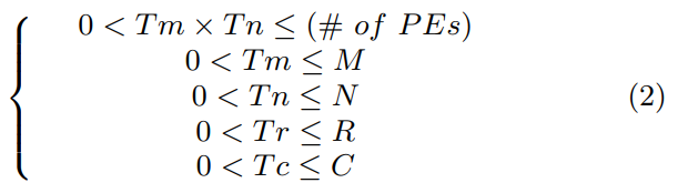
Tile Size Selection
How much size we should tile the feature maps for optimal solution? FPGA has its own hardware computation roof, and we can calculate the computation roof of our implementation using equations below:
Equation 3 in Optimizing FPGA-based Accelerator Design for Deep Convolutional Neural Networks, Chen Zhang et al. FPGA 2015
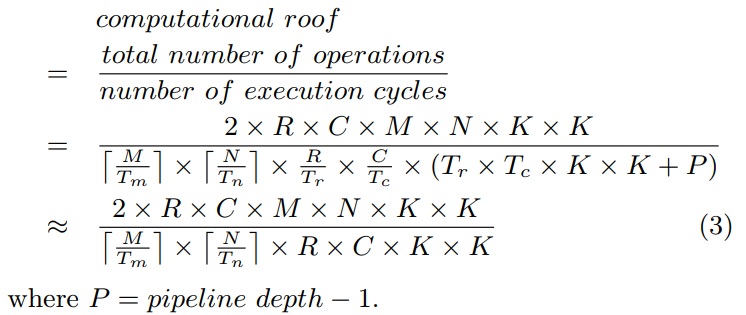
By changing the tiling factor Tm and Tn, we can get optimal tiling factor which maximizes computational roof of our implementation.
And each values are limited as follow:
Equation 2 in Optimizing FPGA-based Accelerator Design for Deep Convolutional Neural Networks, Chen Zhang et al. FPGA 2015
Memory Access Optimization
I can remove Store output feature map partial sums by changing the loading data location in loop statements:
// External Memory transfer
for ( row = 0 ; row < R ; row += Tr ) {
    for ( col = 0 ; col < C ; col += Tc ) {
        for ( oc = 0 ; oc < M ; oc += Tm ) {
            for ( ic = 0 ; ic < N ; ic += Tn ) {
            // Load input feature maps
            // Load kernels

            	// On-chip Memory computation
            }
		// Store output feature map
        }}}
I remove the Load output feature map partial sums and pull the Store output feature maps outside of the input channel iteration loop. I don’t need to load output feature map partial sums because the initial value of output feature maps is 0.
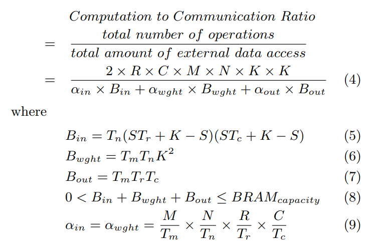
CTC Ratio
We can calculate the CTC Ratio, which is x-axis in Roofline Model, by using tiling factors:
Equation 4 to 9 in Optimizing FPGA-based Accelerator Design for Deep Convolutional Neural Networks, Chen Zhang et al. FPGA 2015
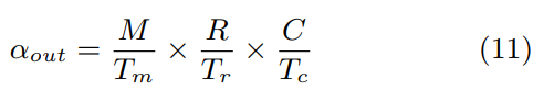
If we apply Memory Access Optimization:
Equation 11 in Optimizing FPGA-based Accelerator Design for Deep Convolutional Neural Networks, Chen Zhang et al. FPGA 2015
Design Space Exploration
We can choose optimal design in the Roofline Model graph:
Equation 8 in Optimizing FPGA-based Accelerator Design for Deep Convolutional Neural Networks, Chen Zhang et al. FPGA 2015
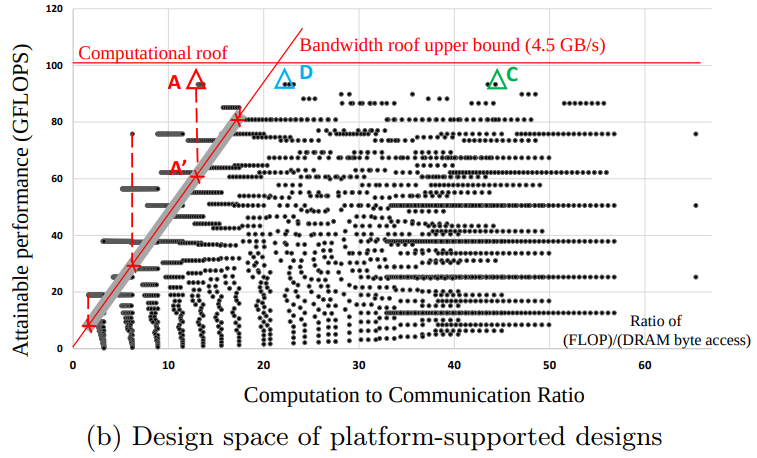
In this case, the design A is actually considered A’ because of the bandwidth limitation. The optimal design is C which has the highest Attainable Performance.
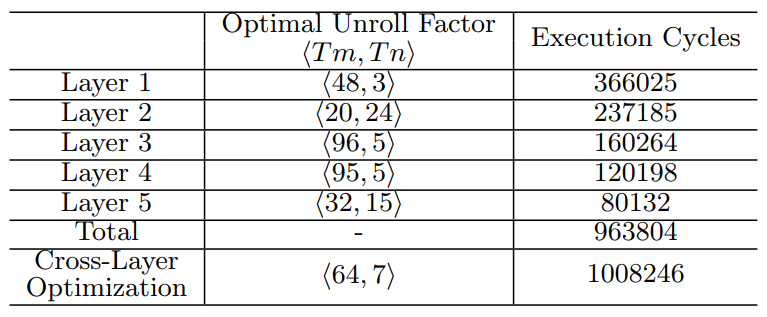
Each layer has its own dimension factors (i.e. R, C, M, N) and tiling factors (i.e. Tr, Tc, Tm, Tn). That is, each layer has its own optimal design which has specific tiling factors. The following table shows the Optimal Unrolling Factor for each layer and total in DNN.
Table 4 in Optimizing FPGA-based Accelerator Design for Deep Convolutional Neural Networks, Chen Zhang et al. FPGA 2015
Implemenataion Details
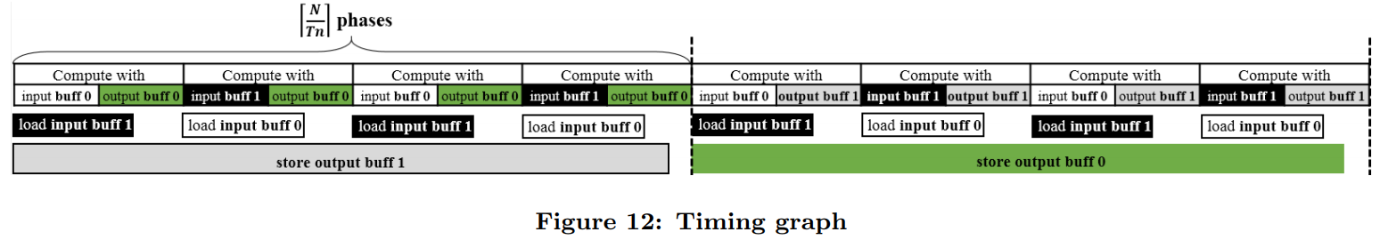
Double Buffering
There is some delays through each steps because of data transfer from memory. To reduce these delays, we can use Double Buffering. One buffer load the data during the other one is consumed by computation units.
Figure 12 in Optimizing FPGA-based Accelerator Design for Deep Convolutional Neural Networks, Chen Zhang et al. FPGA 2015
External Data Transfer Engine
We use IP-AXI to transfer data from External Memory to On-chip Memory. We can use multiple IP-AXI to improve the bandwidth. In single IP-AXI, even though we make the bitwidth wide, the bandwidth isn’t increased. But, if we use a number of IP-AXI, the overall bandwidth is increased.
Figure 13 in Optimizing FPGA-based Accelerator Design for Deep Convolutional Neural Networks, Chen Zhang et al. FPGA 2015
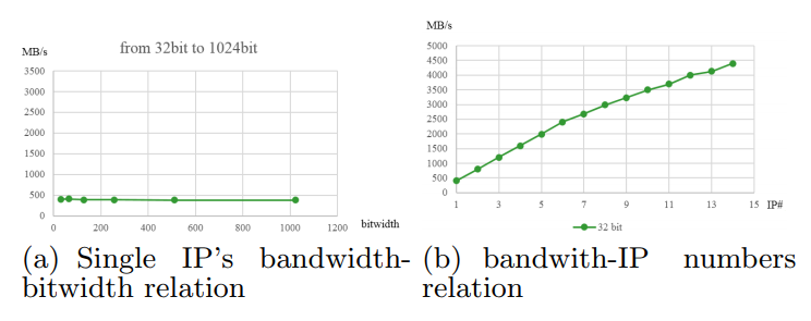
Because the implementation C needs only 1.55 GB/s, we use only 4 IP-AXI to achieve such bandwidth.
Evaluation
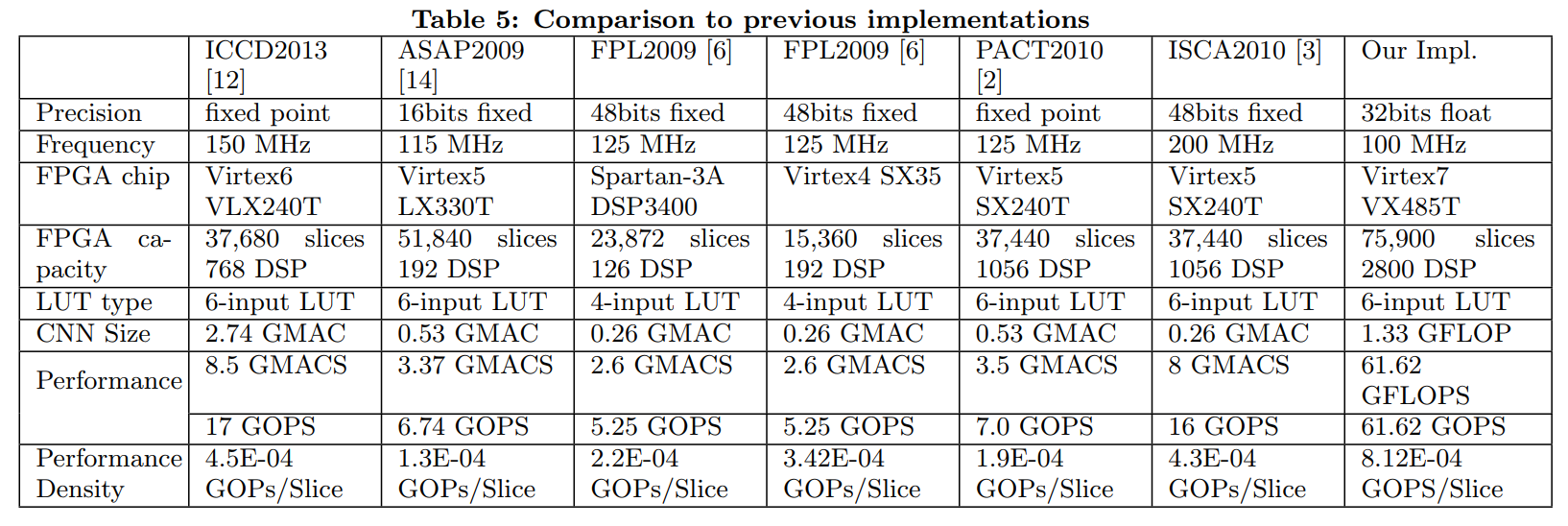
Comparison to previous implementation
Table 5 in Optimizing FPGA-based Accelerator Design for Deep Convolutional Neural Networks, Chen Zhang et al. FPGA 2015
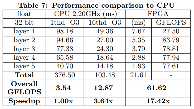
Comparison to CPU
Table 7 in Optimizing FPGA-based Accelerator Design for Deep Convolutional Neural Networks, Chen Zhang et al. FPGA 2015
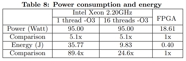
Power Consumption and Energy
Table 8 in Optimizing FPGA-based Accelerator Design for Deep Convolutional Neural Networks, Chen Zhang et al. FPGA 2015